Backside thinning of semiconductor compound wafers such as SiC/GaN.
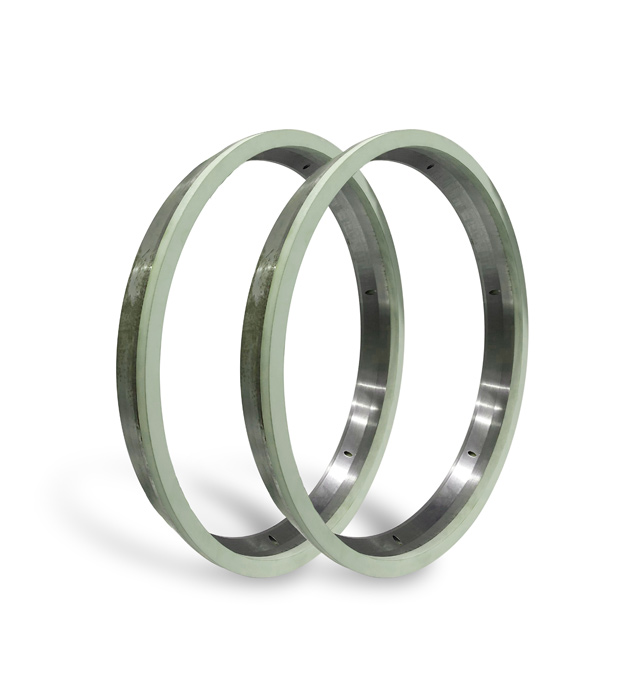
1. By using a new type of porous structure with high abrasive removal capacity to fix abrasive grains, this enables efficient processing and high surface quality for the backside thinning of SiC wafers.
2. The product adopts a new type of nano-scale ceramic base body, featuring high porosity, good sharpness, and excellent cost performance.
3. The product can be matched with different models of grinding machines from both domestic and foreign manufacturers, and can be customized with different grit sizes and specifications according to customer requirements.